| The performance and aggregation structure of High-mobility Polymeric semiconductors | |||||||||||||||||||||||||||||||||||||||
| From: PublishDate:2016-06-03 Hits: | |||||||||||||||||||||||||||||||||||||||
Polymeric semiconductors are the important part for fabricating flexible organic photoelectronic devices. Therefore the development of solution-processible, high mobility polymeric semiconductors is very emergency for fabricating large scale, low-cost organic circuits. In this contribution, a novel design strategy about nonplanar but conjugated BTP-based polymeric semiconductors (PBTP-IDG,PBTP-DPP, and PBTP-NDI, Figure 1) has been reported by Chen and co-workers. By incorporating the nonplanar BTP units into the polymer backbones, the solubility, possibility, aggregation structure, and device performance of the BTP-based polymer semiconductors has been well tuned. The field-effect transistor performance and thin film aggregation structure of the three BTP-based polymers had been investigated. This work had been published in the top journal of Macromolecules (Selected as the Most Read Articles in Macromolecules in April, 2015, Top 25).
Figure 1. Molecular structure of the three BTP-based polymeric semiconductors The bottom-gate bottom-contact OFETs had been fabricated by solution spin-coating technique. Investigation of the OFETs performance indicated that three BTP-based polymer exhibited well hole transport properties in ambient air and excellent ambipolar performance in a N2 glove-box. In ambient air, a high hole mobility of 1.43 cm2 V−1s−1 had been obtained for the PBTP-DPP-based OFETs. When the PBTP-DPP based OFETs were measured in a N2 atmosphere, the well balanced hole and electron mobilities of 0.68 and 0.13 cm2 V−1 s−1 had been demonstrated, respectively. These results suggest that the BTP-based polymeric semiconductors are the promising materials in the field of flexible circuits. Table 1. Performance Parameters for the Polymers-Based OFET devices ( ameasured in ambient air. b measured in a N2 glove-box. )
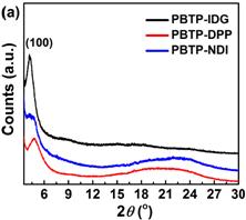
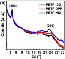
Thin film crystallinity and microstructure are also critical for explaining the differences of OFETs performance, thus the microstructures of the polymers thin films were studied by GIXRD in Beijing Synchrotron Radiation Facility. Figure 2 shows the typical out-of-plane and in-plane diffraction curves of the polymers thin films. Note that the clear (100) diffraction peaks at 2q = 4.25 and 4.50° in out-of-plane patterns, corresponding to the small lamellar-distances of 20.77 and 19.61 Å, were detected for the annealed thin films of PBTP-IDG and PBTP-NDI, respectively. Among the three BTP-based polymers, the smallest lamellar-distance of 18.31 Å was obtained in the PBTP-DPP thin film, which was calculated from (100) diffraction signal at 2q = 4.82° in out-of-plane patterns. This close lamellar stacking can facilitate high performance charge transport. Note that (100) diffraction peaks can be observed in both out-of-plane and in-plane diffraction patterns, suggesting that a kind of mixture stacking microstructures existed in the three BTP-based polymer thin films. However, (010) diffraction peaks can be observed clearly from in-plane patterns. It can be concluded that three polymers take mainly edge-on orientation respective to substrates. This kind of stacking microstructure is similar with many high performance polymers. On the basis of the data obtained from in-plane patterns, PBTP-DPP thin films exhibited a (010) feature at 2q = 24.4°, with a close π–π stacking distance of 3.64 Å, which was smaller than those of PBTP-IDG (3.69 Å) and PBTP-NDI (3.83 Å) thin films. This close π–π stacking structure would provide an effective channel for charge carrier transport.
Figure 2. Out-of-plane (a) and in-plane (b) GIXRD patterns of the polymers thin films annealed at 220 °C. Article: Chao Li, Zupan Mao, Huajie Chen,* Liping Zheng, Jianyao Huang, Bin Zhao, Songting Tan, and Gui Yu.* Synthesis, Characterization, and Field-Effect Transistors Properties of Novel Copolymers Incorporating Nonplanar Biindeno[2,1-b]thiophenylidene Building Blocks. Macromolecules, 2015, 48 (8), 2444–2453.
|
|||||||||||||||||||||||||||||||||||||||
|
|
|||||||||||||||||||||||||||||||||||||||
| Chinese
- Beamline 1W1 of BSRF started to runoperate in the couplingparasitic mode of BEPCII
- Synthesis of High Performance Polymer Materials for Field Effect-Transistors
- Surfactant molecular aggregates in green solvents
- GIXRD has played an important role in the characterization of organic thin-film transistors
Copyright © 2011 - 2012 Beijing Synchrotron Radiation Facility


