| Defect Engineering in Two Common Types of Dielectric Materials for Electromagnetic Absorption Applications |
| From: PublishDate:2020-07-31 Hits: |
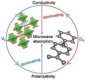
Dielectric materials are greatly desired for electromagnetic absorption applications. Lots of research shows that conduction loss and polarization are two of the most important factors determining complex permittivity. However, the detailed dissipation mechanisms for the improved microwave absorption performance are often based on semiempirical rules, lacking practical data relationships between conduction loss/polarization and dielectric behaviors. A team from Nanjing University of Aeronautics and Astronautics has gained insight into the dissipation mechanisms of dielectric microwave absorption materials. Their research has been published on May 8th, 2019 in Advanced Functional Materials. Here, a strategy of introducing point defects is used to understand such underlying relationships, where polarizability and conductivity are adjustable by manipulating oxygen deficiency or heteroatoms. Based on first principles calculations and the applied oxygen-deficient strategy, dielectric polarization is shown to be dominant in determining the permittivity behaviors in semiconductors. Meanwhile, the presented nitrogen doping strategy shows that conduction loss is dominant in determining the permittivity behavior in graphitized carbon materials.
Given that it is difficult to operate and evaluate the practical polarization process in alternating electromagnetic field at GHz, we still could not present experimental evidence to illustrate the detailed dielectric polarization process. Here, the chemical environments around C after nitrogen doping were detected by near edge X-ray absorption fine structure (NEXAFS) experiments carried out at BSRF. Near-edge X-ray absorption occurs when the core electron is excited to an unoccupied state. The spectra are characterized by four main features: the edge (atomic contribution at about 284.6 eV), a structure characterized by two peaks at 286.1 and 288.6 eV, a shoulder at about 292.4 eV, and a large magnetic spin (MS) resonance centered at about 307 eV, which are labeled as A, B, C, and D in all spectra, respectively. The B peak is assigned to free-electron-like interlayer states in graphite or carbon nanotubes. As can be seen from the NEXAFS spectra, the presence of a pronounced B peak indicates structural changes with the increased sp3-like structure, while the decreased intensity of A peaks demonstrates a weakening of the C-C π * network. The changes of microscopic chemical environments/electrical states indicate the influence of nitrogen doping on the dielectric polarization process in graphitized carbon. The validity of the methods for using point defects to explore the underlying relations between conduction loss/polarization and dielectric behaviors in semiconductor and graphitized carbon are demonstrated for the first time, which are of great importance in optimizing the microwave absorption performance by defect engineering and electronic structure tailoring. Article:
B. Quan, W. H. Shi, S. J. H. Ong, X. C. Lu, P. L. Y. Wang, G. B. Ji, Y. F. Guo, L. R. Zheng, Z. C. J. Xu, Defect Engineering in Two Common Types of Dielectric Materials for Electromagnetic Absorption Applications. Advanced Functional Materials, 2019, 29 (28), 1901236. |
|
|
| Chinese

News and Events
- Metal-free efficient photocatalyst for stable visible water splitting——Top ten major scientific progresses in China in 2015
- The nano-resolution imaging platform was awarded the first rate prize of Beijing Science and Technology in 2014
- Beamline 1W1 of BSRF started to runoperate in the couplingparasitic mode of BEPCII
- Synthesis of High Performance Polymer Materials for Field Effect-Transistors
- Surfactant molecular aggregates in green solvents
- GIXRD has played an important role in the characterization of organic thin-film transistors

Copyright © 2011 - 2012 Beijing Synchrotron Radiation Facility